Physical AI for the semiconductor back end
Every package, perfectly bonded.
Chipira is the autonomous operations layer for advanced packaging. It perceives every die, bond and stack, decides inside an approved envelope, and writes back to the tools — across bonders, molding, inspection and test, whoever built them.
Connector coverage across the back end
- ASMPT
- BESI
- Kulicke & Soffa
- EV Group
- SUSS MicroTec
- TOWA
- Nordson
- Camtek
- Onto Innovation
- Advantest
- Teradyne
- Cohu
Vendor-neutral integration over SECS-GEM, tool APIs and OT interfaces. Vendors listed are integration targets for the connector library and are not endorsements or commercial partnerships.
The problem
The bottleneck moved to the back end
The AI boom does not only run on chips. It runs on advanced packaging — the back-end step where finished dies are bonded, stacked and interconnected into the modules behind every accelerator, HBM stack and phone. That step has become the single biggest capacity and yield risk in the semiconductor supply chain.
Inside an OSAT, known-good dies and chiplets are diced, placed and bonded onto interposers or substrates by die-attach, flip-chip or — increasingly — hybrid bonding, where two surfaces are joined copper pad to copper pad with sub-micron alignment and zero tolerance for particles. They are then stacked, underfilled, molded and tested. It is a nanometre-to-micron craft run at brutal cost.
One warped panel, one void beneath a bump, one cracked die, one misaligned hybrid bond, one particle — and a package worth thousands of dollars, carrying already-expensive known-good die, is gone. Warpage, bond-line thickness, void formation and co-planarity all drift with material lot, temperature and panel. 2.5D, 3D and hybrid-bonding yields ramp slowly and painfully. Each new package design costs quarters of manual tuning.
And the people who govern that ramp — packaging process and yield engineers — are among the scarcest talent in the industry. Most lines still run on manual recipe tuning, rule-based inspection and reactive yield firefighting, with tools from a dozen vendors sitting under one roof and none of them talking to each other.
By the numbers
The economics of a back-end defect
- $30B Advanced-packaging automation, process control, inspection, test and fab software — the market Chipira sits inside.
- ~16% Annual growth, pulled by the AI-accelerator, HBM and chiplet transition.
- 12-high DRAM dies in a current HBM stack, joined through thousands of through-silicon vias. Any one of them can end the package.
- Quarters Typical manual tuning time to ramp a new package design or node to target yield.
Market figures are Chipira’s own estimates of the addressable opportunity, drawn from public equipment, inspection, test and fab-software segment data. Treat them as an internal view, not a research-house citation.
What the platform does
Perception, control and simulation — on the same line
Three of the seven agents, shown as they appear to a process engineer standing at the tool.
Warpage-and-Defect
It sees the void before it costs you a package
Fine-tuned vision models run at the fab edge across X-ray and CT volumes, SAM maps and AOI images — classifying voids, warpage, bump bridging, die cracks and delamination in one perception layer instead of five vendors’ fixed thresholds. Every call is grounded, cited to a standard, and logged.
Meet the agents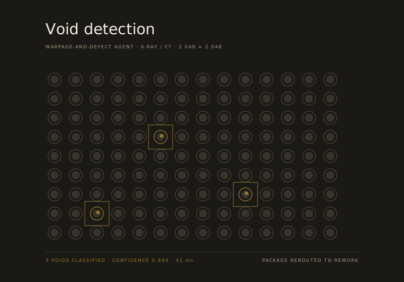
Stack-and-TSV
It sequences the stack so the best die never goes to waste
HBM and chiplet stacking is a sequencing problem with enormous stakes: place a good die on a compromised stack and you lose both. Chipira orders known-good die, plans TSV and underfill, and holds the stack inside a thermal and mechanical envelope it has already validated in simulation.
Read about Stackon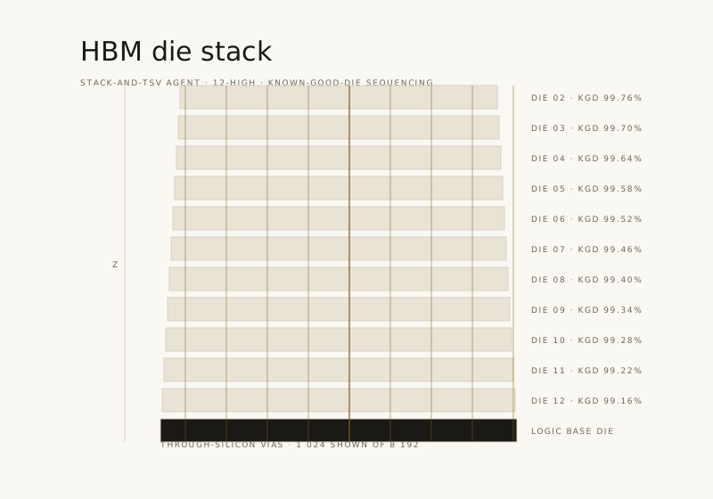
Package-and-line twin
It hits the spec before the line ever runs
Every proposed move — a recipe change, an alignment correction, a new stacking order — is first executed in a package-and-line twin that simulates bonding, stacking and molding. The twin returns a predicted warpage, void and yield outcome. Only then does the move reach a tool.
How the twin works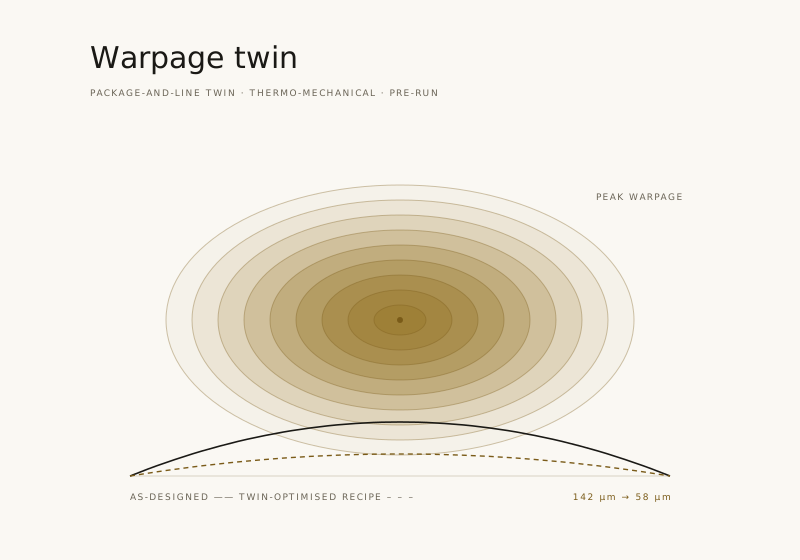
Process integration leadTier-one OSAT, advanced packagingOur inspection tools measure beautifully. They just cannot do anything about what they see.
Composite drawn from design-partner and industry conversations. Illustrative, not a customer endorsement.
The loop
Perceive. Decide. Act. Verify.
Incumbents stop at measurement or hold a setpoint. Chipira closes the loop — and every supervised correction becomes training data.
-
Perceive the die, substrate and package
X-ray and CT volumes, SAM maps, AOI images, alignment metrology, force, temperature, cure and test telemetry are time-aligned into one view of the package as it is actually being built.
-
Plan the place, bond, stack, mold and test
The orchestrator proposes the placement, bond profile, stacking order, underfill and test route, then checks the whole plan in the package-and-line twin against the target warpage, void and yield spec.
-
Act inside an approved envelope
Setpoints are written back to bonders, aligners, molding tools and handling robots over SECS-GEM and vendor APIs — bounded by action envelopes your engineers define, with fail-safe stop and rollback.
-
Verify, log and retrain
Inspection and test outcomes verify what actually happened. Every recommendation, approval, write-back, exception, rollback and result lands in an immutable, yield-grade audit trail — and trains the next model.
The agents
Seven agents under one packaging-fab orchestrator
Each is separately buyable and separately provable. Together they are the loop.
-
01
Place-and-Bond
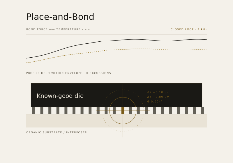
Runs die-attach, flip-chip and hybrid bonding — placement accuracy, bond force, thermal profile and sub-micron alignment, held inside an approved action envelope.
-
02
Stack-and-TSV
Optimises HBM and chiplet die-stacking, through-silicon-via sequencing and known-good-die ordering so the most valuable die is never spent on a doomed stack.
-
03
Warpage-and-Defect
Senses and predicts warpage, voids, bump co-planarity and bridging, die cracks and delamination across X-ray/CT, SAM and AOI — one perception layer, not five thresholds.
-
04
Mold-and-Underfill
Controls molding, underfill flow and cure to eliminate voids and residual warpage before the package is committed to test.
-
05
Substrate-Handling
Drives robotic die, substrate and panel handling and cassette logistics, keeping particles and mishandling out of the bond.
-
06
Test-and-Bin
Runs final and system-level test and binning, closing the loop between what was bonded and what actually works.
-
07
Yield-and-Ramp
Fuses defect root-cause, tool health and yield analytics into the decisions that shorten a ramp from quarters to weeks.
The console
Autonomy your engineers can supervise
Chipira never asks a fab to trust a black box. Exceptions surface with confidence, evidence and a recommended action; the engineer approves, corrects or overrides — and the correction becomes training signal.

Who we build for
Three people have to believe it
Economic buyer
Packaging fab & operations director
Owns yield, ramp, throughput and cost. Wants a higher-yielding, faster-ramping line without hiring process engineers who do not exist on the market.
- Yield and ramp time
- Warpage and void scrap
- Known-good-die loss
- Throughput and labour
Champion
Process integration & yield engineer
Owns bonding, stacking and molding process, defect reduction and yield ramp. Wants relief from recipe firefighting and a real root cause instead of a threshold alarm.
- Autonomous bonding and stacking
- Defect root-cause in minutes
- Recipe drift held automatically
- Craft captured, not lost
Approver
Quality, reliability & IT/OT
Owns warpage and void quality, package reliability, binning, field returns — and the security and process-IP posture that lets any of it happen.
- Yield-grade audit trail
- Per-tenant data isolation
- Process-IP protection
- On-premise deployment option
How an engagement starts
Narrow, measured, paid
We do not sell a platform migration. We sell one workflow with one number attached to it.
- 01 — Shadow mode
- Chipira instruments your wedge workflow and runs alongside the line without touching it. You get a measured baseline of yield, scrap and ramp before anything changes.
- 02 — Assist mode
- The agent recommends bonding, molding and alignment moves and classifies defects; your engineer approves each one. Accuracy is proven against the engineer plus the existing inspection baseline.
- 03 — Graduated autonomy
- Low-risk moves execute automatically inside approved action envelopes, validated in the twin. Exceptions escalate; unsafe or out-of-spec moves roll back.
- 04 — Expansion
- Once the agreed metric is met, adjacent modules on the same package flow come online — then the next line, then the next fab.
Before you ask
The four questions every fab asks first
-
No, unless you explicitly contract for it. Chipira runs inference at the fab edge on your premises, with per-tenant data and model isolation. Federated aggregate model updates are opt-in and contractual; an air-gapped deployment is available for sensitive lines.
-
It escalates. Every action is bounded by an action envelope your engineers define, validated against the package-and-line twin, and reversible. High-impact and yield-critical decisions sit behind a human-in-the-loop checkpoint until measured accuracy earns more autonomy.
-
Chipira is deliberately vendor-neutral. Connectors target die bonders, hybrid-bonding aligners, molding and underfill tools, X-ray/CT, SAM and AOI systems, test cells and MES over SECS-GEM, vendor APIs and OT interfaces — read and, where you allow it, write-back.
-
Because you defined the number before we started. A pilot carries a signed success metric — classification accuracy against your baseline, yield points, scrap reduction, known-good-die loss or ramp weeks — and the audit trail proves what the agent did.
Start narrow, expand relentlessly
Land one workflow. Own the loop.
A Chipira engagement begins with a single wedge workflow, a shadow-mode baseline and one signed success metric. Everything after that is expansion.